What is PCB in electronics
A printed circuit board (PCB) is a fundamental component in modern electronics. It serves as a mechanical base to hold and connect the components of an electric circuit, allowing for the creation of complex electronic system.
What is a PCB?
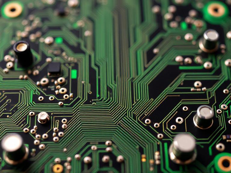
A Printed Circuit Board (PCB) is an electronic assembly that uses copper conductors to create electrical connections between components. It provides mechanical support for electronic components, allowing a device to be mounted in an enclosure. Altium
PCBs are the backbone of most electronic devices, enabling the functionality of everything from simple gadgets to complex computing systems.
Types of PCBs
PCBs come in various types, each suited for specific applications:
Single-Layer PCBs
-
Contain only one layer of conductive material.
-
Used in simple electronic devices.VECTOR BLUE HUB+3Wikipedia+3pcbcart.com+3Informa TechTarget+1YouTube+1
Double-Layer PCBs
-
Have conductive material on both sides.
-
Allow for more complex circuits.resources.pcb.cadence.com+3Ansys | Engineering Simulation Software+3Wikipedia+3Informa TechTarget
Multi-Layer PCBs
-
Consist of multiple layers of conductive material separated by insulating layers.
-
Used in advanced electronics like computers and medical devices.Wikipedia
Rigid PCBs
-
Made from solid substrate materials.
-
Provide strength and rigidity.Wikipedia+4Altium+4Informa TechTarget+4
Flexible PCBs
-
Made from flexible materials.
-
Can bend and twist, suitable for wearable devices.Esprit Electronics+7pcbcart.com+7Wikipedia+7
Rigid-Flex PCBs
-
Combine rigid and flexible board technologies.
-
Used in applications requiring both flexibility and rigidity.Electronics-Lab.com+18Informa TechTarget+18Wikipedia+18
PCB Materials and Layers
PCBs are composed of several materials and layers:Informa TechTarget
Substrate
-
The base material, usually fiberglass, provides mechanical support.Altium
Copper Layer
-
Conductive layer that forms the circuit paths.ABL Circuits+1Wikipedia+1
Solder Mask
-
Protective layer that prevents solder bridges.
Silkscreen
-
Used to add labels and markings for component placement.
The number of layers in a PCB can vary depending on the complexity of the circuit. Multi-layer PCBs allow for more intricate and compact designs.
PCB Manufacturing Process
The manufacturing of PCBs involves several steps:Ansys | Engineering Simulation Software+1pcbcart.com+1
1. Design and Layout
-
Creating the schematic and layout using CAD software.
2. Printing the Design
-
Transferring the design onto the PCB substrate.
3. Etching
-
Removing unwanted copper to reveal the circuit pattern.
4. Drilling
-
Creating holes for component leads and vias.ABL Circuits+3Wikipedia+3Altium+3
5. Plating and Coating
-
Applying protective coatings and plating the holes.
6. Solder Mask Application
-
Adding the solder mask to prevent solder bridges.
7. Silkscreen Printing
-
Adding component labels and markings.
8. Cutting and Profiling
-
Cutting the PCB to its final dimensions.
9. Testing
-
Conducting electrical tests to ensure functionality.
Applications of PCBs
PCBs are integral to numerous industries and applications:
-
Consumer Electronics: Smartphones, tablets, and home appliances.
-
Automotive: Control systems, navigation, and entertainment systems.
-
Medical Devices: Diagnostic equipment and monitoring devices.
-
Industrial Equipment: Machinery control systems and automation.
-
Aerospace: Navigation systems and communication devices.Ansys | Engineering Simulation Software
Wintech's PCB Solutions

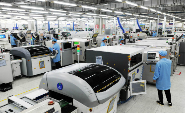
Wintech is a full turnkey service provider specializing in high-mix, low to mid-volume electronics manufacturing and custom material solutions. With a proven track record, Wintech offers state-of-the-art solutions to a global customer base.
Services Offered:
-
- PCB Design & Layout
- PCB Manufacturing
- PCB Assembly & PCBA SMT
- Quick Turn Fast PCB Prototype Assembly
- New Product Introduction NPI
- Plastic Molding
- Metal Precision Machining
Wintech's commitment to quality and customer satisfaction makes it a reliable partner for electronic manufacturing solutions.
Summary Table
| Aspect | Details |
|---|---|
| Definition | A board that connects electronic components using conductive pathways. |
| Types | Single-layer, double-layer, multi-layer, rigid, flexible, rigid-flex. |
| Materials | Fiberglass substrate, copper layers, solder mask, silkscreen. |
| Manufacturing Steps | Design, printing, etching, drilling, plating, solder mask, silkscreen, testing. |
| Applications | Consumer electronics, automotive, medical, industrial, aerospace. |
| Wintech Services | Design, manufacturing, assembly, prototyping, NPI, molding, machining. |


