PCB Board Production Process
Table of Contents
-
Introduction to PCB Board Production
- What is a PCB (Printed Circuit Board)?
- Why PCBs are Essential in Electronics
-
Steps in PCB Board Production Process
- Step 1: PCB Design and Layout
- Step 2: PCB Material Selection
- Step 3: PCB Fabrication
- Step 4: PCB Assembly
- Step 5: Inspection and Testing
- Step 6: PCB Packaging and Delivery
- Benefits of Choosing a Professional PCB Manufacturing Service
- Common Challenges in PCB Production
- FAQ (Frequently Asked Questions)
- Conclusion
- PCB Board Production Table
Introduction to PCB Board Production
What is a PCB (Printed Circuit Board)?
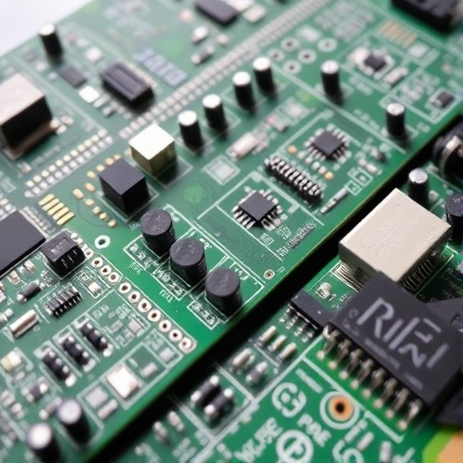
A Printed Circuit Board (PCB) is a fundamental component in most electronic devices. It provides both mechanical support and electrical connectivity for electronic components. PCBs are used in everything from smartphones and computers to medical devices and automotive electronics. The PCB houses the circuit and the electronic components like capacitors, resistors, and transistors.
In the modern world, Wintech Technology Co., Ltd. stands as one of the leading providers of Electronics Manufacturing Services (EMS), delivering a comprehensive range of services that include PCB design, manufacturing, assembly, and SMT (Surface-Mounted Technology). Wintech was founded in 1995, and over the years, it has expanded significantly, surpassing USD $120 million in fiscal year 2019 and employing more than 1,000 people.
As an ODM provider, Wintech offers one-stop contract manufacturing services for industries such as medical, telecommunications, automotive, lighting, aerospace, and technology. Their expertise in PCB manufacturing is crucial for many of these industries, where precision and reliability are key.

Steps in PCB Board Production Process
The process of PCB board production involves several critical stages. These stages must be carefully followed to ensure the final product meets the required specifications and quality standards. Let’s break down the PCB manufacturing process into its key steps:
Step 1: PCB Design and Layout

The first step in the PCB production process is PCB design. This step involves the creation of a digital layout that defines the electrical connections between components. The layout will also define the physical placement of pads, traces, and vias, which are the holes that connect different layers of the PCB.
Key Activities in PCB Design:
- Schematic Design: The schematic is the blueprint that shows all the electrical components and their connections.
- PCB Layout: Using the schematic, the components are placed on a virtual PCB, and the connections (traces) are routed.
- Design for Manufacturability (DFM): This is a critical step to ensure that the design can be efficiently manufactured without any issues.
Modern PCB design software like Altium Designer, Eagle, and KiCad are used to create and optimize these layouts.
Step 2: PCB Material Selection

Once the PCB design is complete, the next step is selecting the materials used to manufacture the board. This is crucial because the materials affect the PCB’s performance, durability, and cost.
Common PCB Materials include:
- FR4 (Fiberglass): The most widely used material due to its balance of performance and cost.
- CEM1/CEM3: These materials are often used for low-cost, single-layer PCBs.
- Polyimide: Ideal for flexible PCBs, commonly used in applications like wearable electronics.
Selecting the right material depends on factors such as:
- Operating Temperature Range
- Electrical Conductivity
- Mechanical Strength
- Cost Efficiency
Step 3: PCB Fabrication

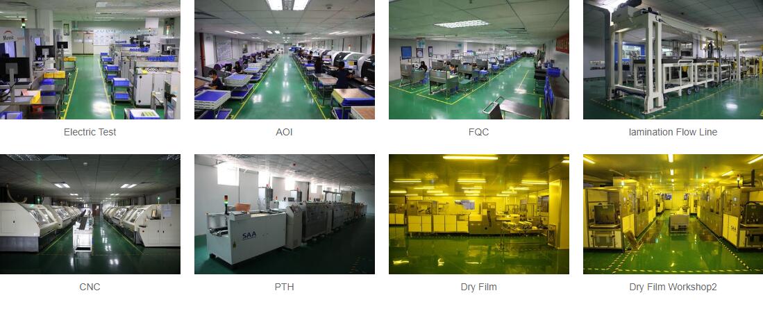
After the design and material selection, the PCB enters the fabrication stage, which involves several complex processes:
- Layering: Multiple layers of copper foil and substrate are stacked together.
- Drilling: Holes are drilled for vias, which are the paths connecting different layers of the PCB.
- Copper Cladding: Copper is then laminated onto the board.
- Etching: The copper is etched away to form the desired circuit traces.
- Solder Masking: A layer of protective mask is applied to prevent soldering issues during the assembly process.
The PCB fabrication process is highly precise, as even small errors can lead to malfunctioning boards.
Step 4: PCB Assembly

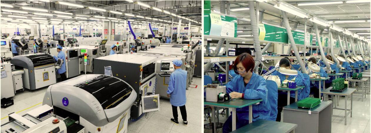
The PCB assembly (also known as PCBA) stage involves placing the electronic components onto the PCB. There are two main methods of assembly:
- Surface Mount Technology (SMT): This is the most common method where components are mounted directly onto the surface of the PCB.
- Through-Hole Technology: Components are inserted into holes drilled through the PCB, and the leads are soldered on the opposite side.
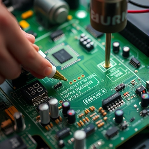
After the components are placed, they are soldered to create electrical connections. Wave soldering and reflow soldering are common methods used in this process.
Step 5: Inspection and Testing

Once the assembly is complete, the PCB undergoes rigorous testing to ensure it meets the required standards.
There are several types of testing, including:
- Automated Optical Inspection (AOI): Uses cameras to detect physical defects.
- In-Circuit Testing (ICT): Tests the electrical performance of individual components on the PCB.
- Functional Testing: Verifies the overall functionality of the PCB in a real-world scenario.
This is the stage where potential errors are identified and corrected to ensure the PCB performs optimally.
Step 6: PCB Packaging and Delivery
Once the PCBs have passed the inspection, they are packaged and prepared for delivery to the client. The packaging must ensure that the PCBs remain static-free and protected during shipping.
Some companies, like Wintech, offer quick-turn PCB prototype assembly services to rapidly produce small batches for testing or small-scale production runs.
Benefits of Choosing a Professional PCB Manufacturing Service
When considering PCB production, working with an experienced provider like Wintech Technology Co., Ltd. offers numerous benefits:
- High-Quality Production: Professional manufacturers use the latest technology and high-quality materials to ensure durable and reliable PCBs.
- Custom Solutions: With capabilities in custom PCB design, Wintech can create solutions tailored to specific needs, whether for automotive, medical, or consumer electronics.
- Cost-Efficiency: A dedicated manufacturer can help reduce overall costs by optimizing the design for manufacturability and ensuring efficient production processes.
- Faster Time to Market: With years of experience and a streamlined process, professional manufacturers can produce PCBs faster, helping companies get their products to market more quickly.
Common Challenges in PCB Production
While the PCB production process is well-established, there are several challenges that manufacturers must overcome:
- Design Complexity: As technology advances, PCB designs become more intricate, which can increase the risk of errors.
- Material Costs: High-quality materials can be expensive, and finding a balance between performance and cost is essential.
- Component Availability: Some electronic components may have limited availability, affecting production timelines.
- Quality Control: Ensuring that every PCB is defect-free can be a challenge, especially in high-volume production runs.
FAQ (Frequently Asked Questions)
1. How long does it take to manufacture a PCB?
- The timeline depends on the complexity of the design and the production volume. Simple prototypes may take 1-2 weeks, while mass production could take several weeks.
2. What is the difference between SMT and through-hole assembly?
- SMT involves placing components directly on the surface of the PCB, while through-hole assembly inserts components through drilled holes for more mechanical strength.
3. Can I get a prototype PCB made before mass production?
- Yes, most PCB manufacturers, like Wintech, offer quick-turn prototype services, allowing you to test and validate the design before moving to large-scale production.
Conclusion
PCB board production is a complex yet essential process in modern electronics manufacturing. Whether you’re designing for medical devices, automotive systems, or consumer electronics, working with a reliable PCB manufacturer like Wintech Technology Co., Ltd. ensures high-quality, cost-effective, and timely solutions. The steps involved—from design and material selection to assembly and testing—require careful attention to detail to ensure the end product meets your specifications and standards.
PCB Board Production Table
| Step | Description |
|---|---|
| Step 1: Design and Layout | Create schematic and physical layout of the PCB. |
| Step 2: Material Selection | Choose the appropriate materials for the PCB based on design requirements. |
| Step 3: Fabrication | Fabricate the PCB through drilling, copper cladding, and etching processes. |
| Step 4: Assembly | Place and solder components on the PCB using SMT or through-hole technology. |
| Step 5: Inspection & Testing | Conduct various tests like AOI, ICT, and functional testing to ensure the PCB works. |
| Step 6: Packaging & Delivery | Package and ship the PCB with appropriate protection for delivery. |
By following these steps and collaborating with experienced manufacturers like Wintech
, companies can produce reliable and functional PCBs that meet the demands of modern electronic applications.


